Benjamin Iñiguez
Biography:
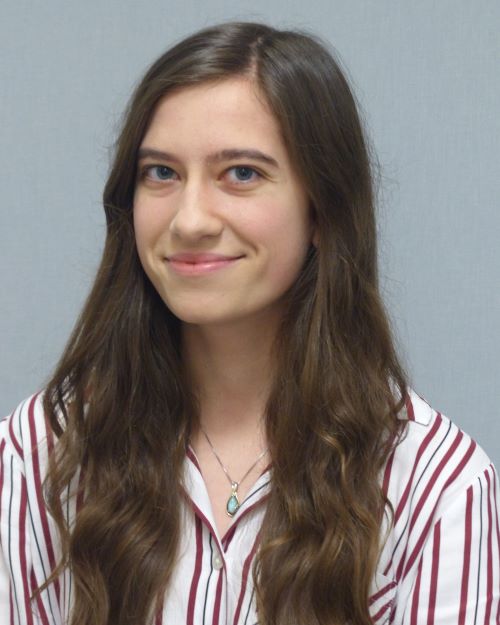
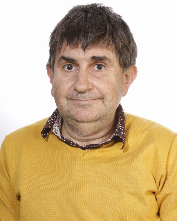
Benjamin Iñiguez obtained the Ph D in Physics in 1992 and 1996, respectively, from the Universitat de les Illes Balears (UIB). His Doctoral Thesis targeted the modeling of submicron MOSFETs. From February 1997 to September 1998 he was working as a Postdoctoral Researcher at the Rensselaer Polytecnhnic Institute in Troy (NY, USA), where he addressed the physics and modeling of a-Si:H and poly-Si TFTs. From September 1998 to January 2001 he was working as a Postdoctoral Scientist in the Université catholique de Louvain (Louvain-la-Neuve, Belgium), supported by two Marie Curie Fellowships from the European Commission, and targeting the physics and modeling of thin film SOI MOSFETs. In February 2001 he joined the Department of Electronic, Electrical and Automatic Control Engineering (DEEEiA)of the Universitat Rovira i Virgili (URV), in Tarragona, Catalonia, Spain) as Titular Professor. In February 2010 he became Full Professor at URV. He obtained the Distinction from the Generalitat for the Promotion of University Research in 2004 and the ICREA Academia Award (the highest award for university professors in Catalonia, from ICREA Institute) in 2009 and 2014. He led two research projects funded by the European Union (EU) and has participated or is participating as URV team leader in five more EU-funded projects. He has supervised or co-supervised 19 Ph D students. He has been the Chair Person of five international conferences and workshops devoted to advanced semiconductor devices, as well as five international training courses or summer schools on device modeling.
He is EDS Distinguished Lecturer since 2004, Editor of IEEE T-ED since August 2016. In 2019 he was elected IEEE Fellow. In 2024 he was appointed EDS Vice-President of the Subcommittee of Regions and Chapters. He also was Chair of the EDS Compact Modeling Technical Council (2017-2020), EDS BoG Member at Large since (2018-2022) and Chair of the Spain ED Chapter (2019-2022), and Chair of the EDS Region 8 SRC (2023).
His main research interests are the characterization, parameter extraction and compact modelling of emerging semiconductor devices, in particular nanoscale Multi-Gate MOSFETs GaN HEMTs, organic and oxide Thin-Film Transistors and organic electrochemical sensors. Several of the models he authored or co-authored are available in many commercial Electron Design Automation (EDA) tools, in particular TFT models. He is one of the authors of the ASM GaN HEMT model, selected as standard by the Compact Modeling Coalition in 2017. He has published more than 190 research papers in international journals and more than 180 abstracts in proceedings of conferences.
From may 2024, he is also the academic responsible in the URV of the interuniversitary Master in Semiconductor Desing Engineering and Microelectronic Design.

François Lime
François Lime received the M.S. and Ph.D. degrees from the Institut National Polytechnique de
Grenoble, Grenoble, France, in 2000 and 2004, respectively. From then until December 2008,
he worked as a Postdoctoral Research Associate at the Universitat Rovira I Virgili, Tarragona
(URV), Spain and the Institut de Microélectronique, Electromagnétisme et Photonique (IMEP-
LAHC), Grenoble, France. In January 2009, he joined URV as a Ramon y Cajal researcher, and is
now an associate professor since 2014.
His past research activities concerned the electrical characterization and modelling in the area
of high-k gate dielectrics and strained-silicon devices. His current research interests are the
compact modelling of electronic devices such as multiple-gate MOSFETs and OTFTs, as well as
the electrical characterization of these devices.
Nadine Dersch
Nadine Dersch received her Bachelor of Engineering and Master of Science degrees at the Technische Hochschule Mittelhessen (THM, University of Applied Sciences) Campus Giessen, Germany, in October 2021 and March 2023. From June 2022, she began her work in the Nanoelectronics/Device Modeling group at the THM and initially dealt with the compact modeling of Amorphous Oxide Semiconductor Thin-Film Transistors (AOS-TFT). Subsequently, the topic of efficient circuit simulation of a memristive crossbar array with synaptic weight variability was dealt with as part of the Master's thesis. The focus was on the consideration of Resistive Random Access Memory (RRAM).
Since October 2023 she is pursuing her Ph. D. with the Universitat Rovira i Virgili. Her work focuses on the development of physics-based modeling approaches for memristors, in particular with regard to stochastic switching behavior, and their implementation in hardware-based artificial neural networks.

Eufamer Carabali
Twenty three years ago, I arrived in Spain from Colombia and I settled in Cambrils, where I started my family and began my career as an industrial electromechanical technician. Over time, I validated my studies in technical engineering in industrial electronics; after completing 60 ECTS credits at the School of Industrial Technical Engineers of Barcelona (EUTIB) affiliated with UPC. Later, I continued studying for a master's degree in occupational risk prevention at the Rovira i Virgili University, which I completed in 2013. Subsequently, I completed another master's degree in engineering and technology of electronic systems with access to a PhD, at URV. Finally, in 2020, I began my PhD studies at Rovira i Virgili University, which I am currently pursuing part-time while working as a senior occupational risk prevention technician at Veolia Serveis Catalunya, located in the Zona Franca of the Parc Logistic in Barcelona.
Ermias Telahun Teka
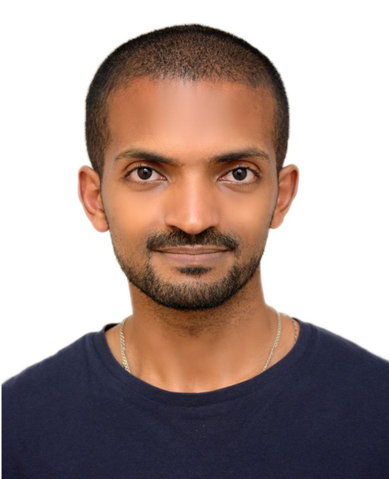
Ermias Telahun Teka obtained his BSc in Electrical (Electronics) Engineering (2015) from Addis Ababa University (AAU), Addis Ababa, Ethiopia and his MSc in Microelectronics Engineering (2020) from AAU. He has worked as an assistant lecturer from August 2015 to December 2020 and as a lecturer from December 2020 to August 2023 at Addis Ababa University. He is currently pursuing his PhD at URV on the Modeling of Organic Neuromorphic devices for biomedical applications.
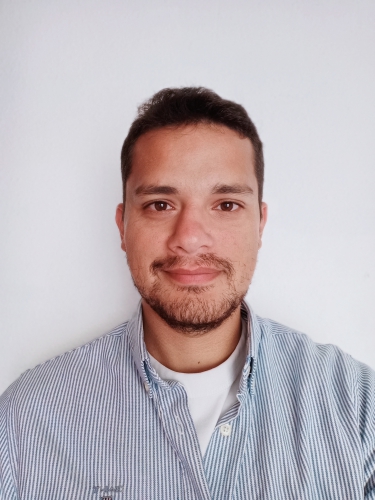
Ahmed Mounir
Ahmed Mounir is currently a PhD researcher at Universitat Rovira i Virgili in Tarragona, Spain. His work focuses on the development of compact models for MoS2 Field-Effect Transistors (FETs), collaborating with Intel and TU Wien. During his PhD, Ahmed completed a research stay at the Microelectronics Institute at TU Wien, furthering his expertise in semiconductor technology. Before his PhD, Ahmed earned a Master of Nanotechnology Engineering from the Arab Academy for Science and Technology in Egypt. This master's program was funded by the European Union's TEMPUS Project, underscoring his commitment to advancing semiconductor device modeling. His research interest is semiconductor device modeling.

