Area 1. Nanoelectronic devices (B. Iñiguez)
- 1. Development of compact models for the new structures of nanodevices, MOS, especially nanoMOSFETs.
- 2. Development of parameter extraction techniques for new compact models of nanodevices.
- 3. Implementation, validation and demonstration of the new compact models of nanodevices in automatic circuit design tools (EDA).
Area 2. Devices for Organic and Large Area Electronics (OLAE) (L.F. Marsal, B. Iñiguez))
- 1. Development of organic device technologies (solar cells and organic thin-layer transistors)
- 2. Understanding the properties of organic materials and amorphous and polycrystalline semiconductors by OLAE devices in microelectronic applications.
- 3. Development of models for OLAE devices.
- 4. Development of device parameter extraction methods for OLAE devices.
- 5. Implementation, validation and demonstration of the new compact OLAE device models in automatic circuit design (EDA) tools.
Area 3. Technology and applications of micro- and nano-porous materials based on silicon and alumina (L. F. Marsal)
- 1. Development of a 2D-D technology of nano and macroporous silicon and self-ordered nanoporous alumina.
- 2. Development of photonic micro and nanostructures. Design and modeling.
- 3. Development of nanophotonic biosensors.
- 4. Micro- and nano-structured substrates for cell growth. Tissue engineering.
- 5. Nanomatrices and nanocapsules for controlled drug administration.
- 6. Nanostructuring of organic and hybrid photovoltaic cells.
Area 4. High-frequency electronic systems (D. Girbau, A. Lázaro)
- 1. Systems for remote sensing of organic pathologies and human vital functions.
- 2. Sensor networks for logistics control, based on RFID technology.
- 3. Development of microwave circuits and systems.
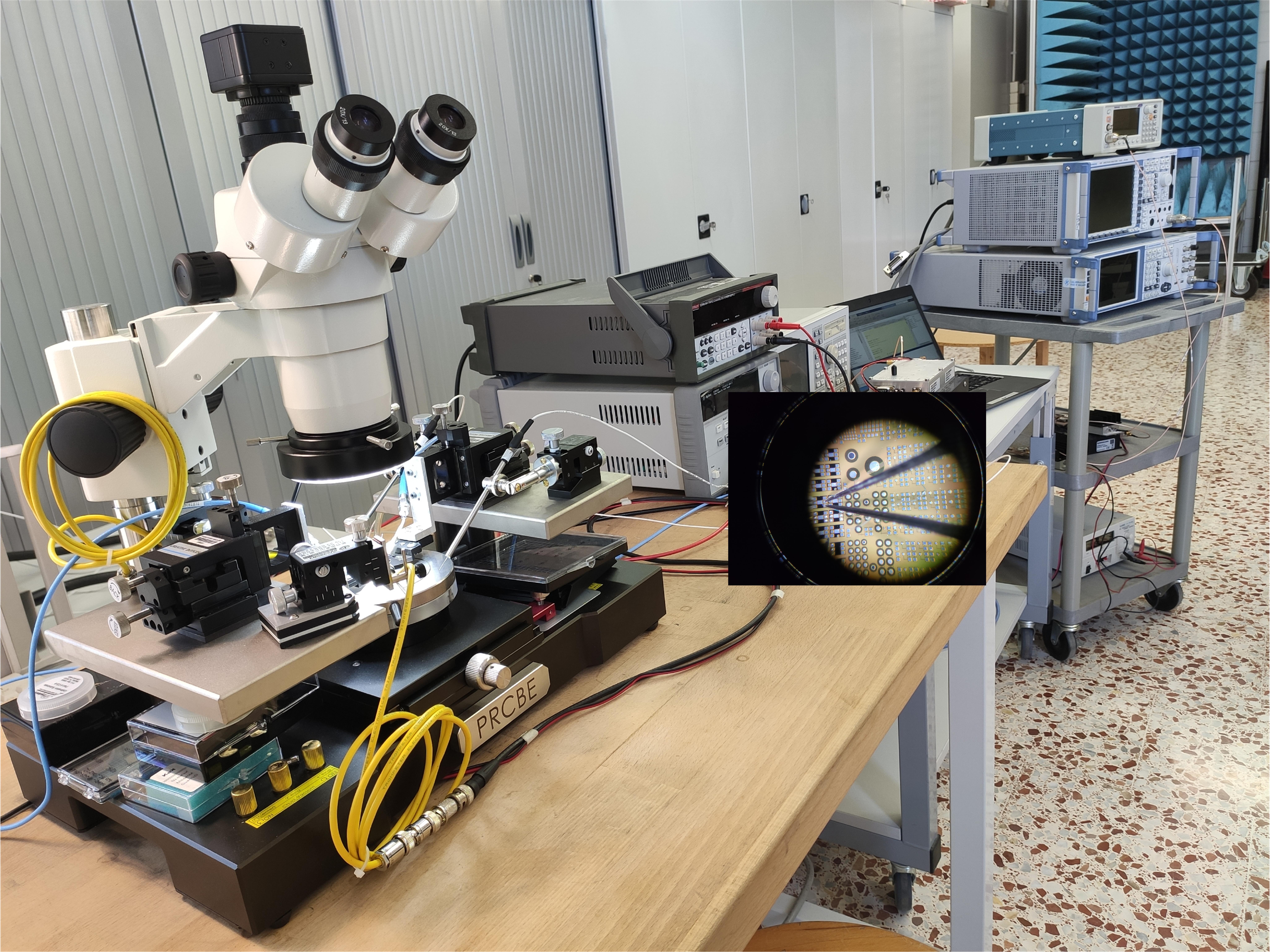
- 4. Development of a characterization system in microwave bands.
Targets
Research objectives in Nanoelectronic Devices
Development of compact models and parameter extraction techniques for new nanodevice structures, mainly MOS and postCMOS type below 12 nm, especially Tunnel FET (TFET) and FETs with different 2D semiconductors. According to the IRDS roadmap, TFETs AND 2D semiconductor FET technologies are very promising for channel lengths below 10 nm. Implementation of models in CAD tools for use in circuit design. A European Horizon Europe project on 2D semiconductor devices will be attempted.
Objectives of the research in Devices for Organic and Large Area Electronics (OLAE)
Development of models for new structures of TFTs, such as Double-Gate OTFTs, OTFTs AND submicron AOS TFTs, Source-Gated OTFTs,...), and for effects some effects not considered adequately so far in organic TFTs and oxides: aging, hysteresis, voltage and temperature stress. Implementation of the models in CAD tools for use in circuit design For this purpose, a project will be requested from a Horizon Europe Call on the design of neuromorphic circuits based on new models of OTFTs transistors, and an MSCA Doctoral Network on TCAD and compact modeling of new OTFT and IGZO TFTs structures. In addition, the group will begin manufacturing printed OTFTs.
Research objectives in Technology and applications of micro- and nano-porous materials based on silicon and alumina
Research in recent years by the NePhoS group has brought the technology of manufacturing nanoporous materials to a level of maturity sufficient to be able to propose devices based on these materials. At the moment there is great control over the properties of materials: geometry, arrangement of pores, effects of interaction with light, optical properties, etc. and efforts are devoted to the definition of applications with impact on society. From 2021, a COST 20126 NETPORE project is being led with the participation of more than 35 countries and 250 researchers. During the next 4 years, different activities will be carried out (training, mobility, workshops, seminars, etc.) and we also have plans to make project proposals within the Horizon Europe framework. The general objective of this Action is the application of nanoporous materials in health, energy and the environment and their transfer and final commercialization. The general objective for the coming years is to achieve two European projects and increase research and development activity in the following activities:
• Biotechnological applications of micro- and nano-structured materials.
- Development of advanced nanophotonic biosensors. The research of the NePhoS Group will focus on optimizing them to achieve minimum detection levels lower than those currently achieved. Functionalization methods, design of nanostructures and intelligent processing of the obtained signals.
- Micro- and nano-structured substrates for cell growth. Nano- and micro-structured materials influence the proliferation, growth and migration of different types of cells. The next objectives will consist of the study for the use of the properties demonstrated to the growth of useful tissues.
- Nanomatrices and nanocapsules for controlled administration of drugs. The nanoporous structure is an ideal platform for drug loading and sustained release. Methods will be studied
of release control based on pore geometry, or molecular gates and intelligent release systems.
• Photovoltaic Energy Conversion and Storage.
The generation of energy from light is one of the research lines of the NePhoS group. The manufacture of efficient organic and hybrid solar cells with efficiencies above 20% and stable over time is an important objective of the group. New organic and nanoporous materials can contribute to the improvement of these characteristics through two main objectives:
- Nanostructuring of organic and hybrid photovoltaic cells. The objective will be to improve the collection of photons, the transport of the carriers to the corresponding electrodes and the efficiency of the collection. Study of devices under indoor lighting conditions for IoT applications.
- Study and modeling of the useful life time of nanostructured organic solar cells. There are currently joint efforts by many groups at European level to achieve the stability necessary for commercialization.
Research objectives in High Frequency Electronic Systems
The High Frequency Electronic Systems line is dedicated to the research and development of devices, circuits and systems in the microwave and millimeter band range. The three target applications of this line of research are biomedical, RFID systems and communication systems. Within this framework, the different activities, specific to an application in some cases and transversal in others, in which the tasks currently carried out and in the coming years are subdivided are the following:
- 1 Sensor networks and IoT:
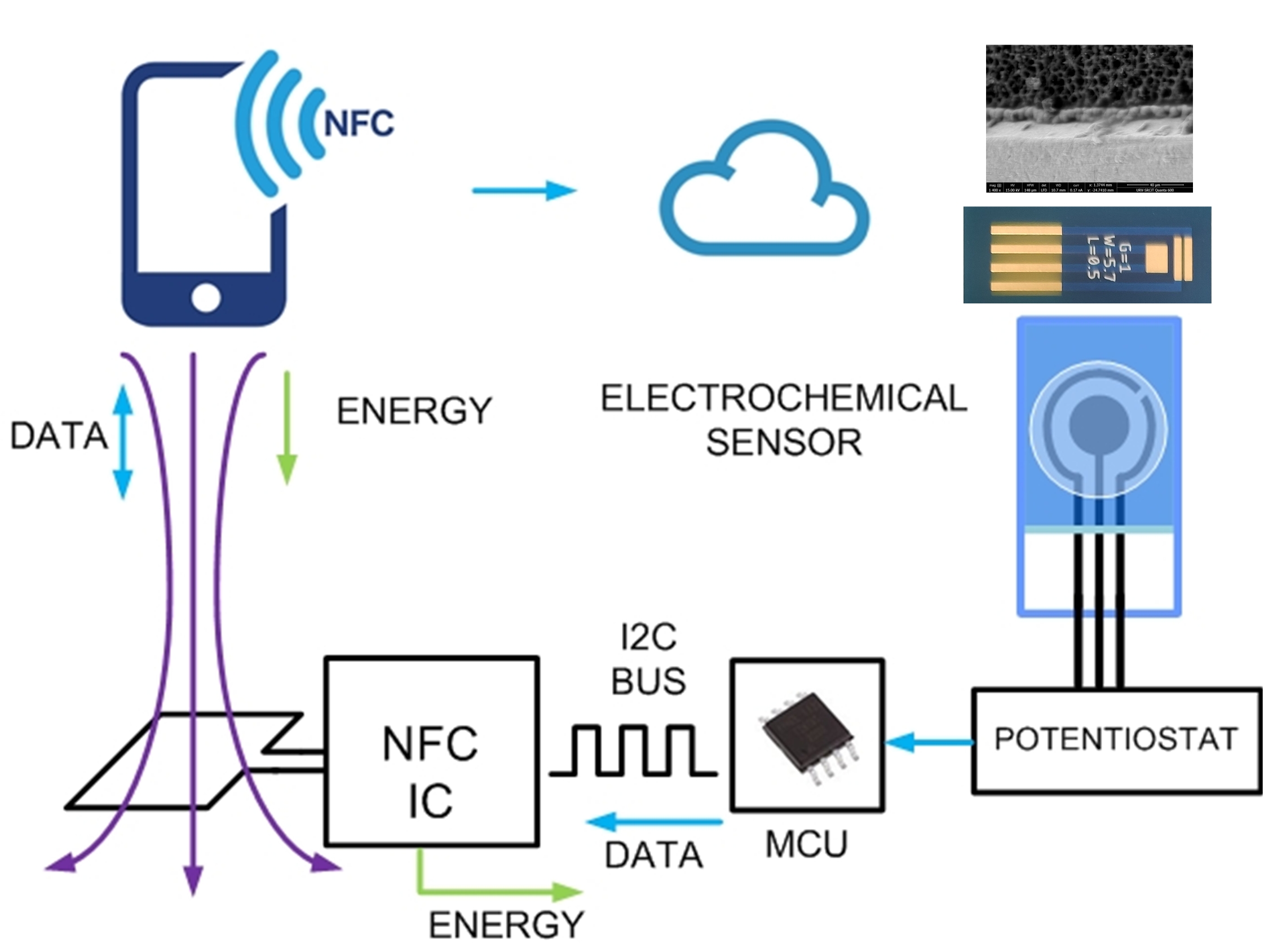
- Sensors based on Near Field Communication (NFC) technology.
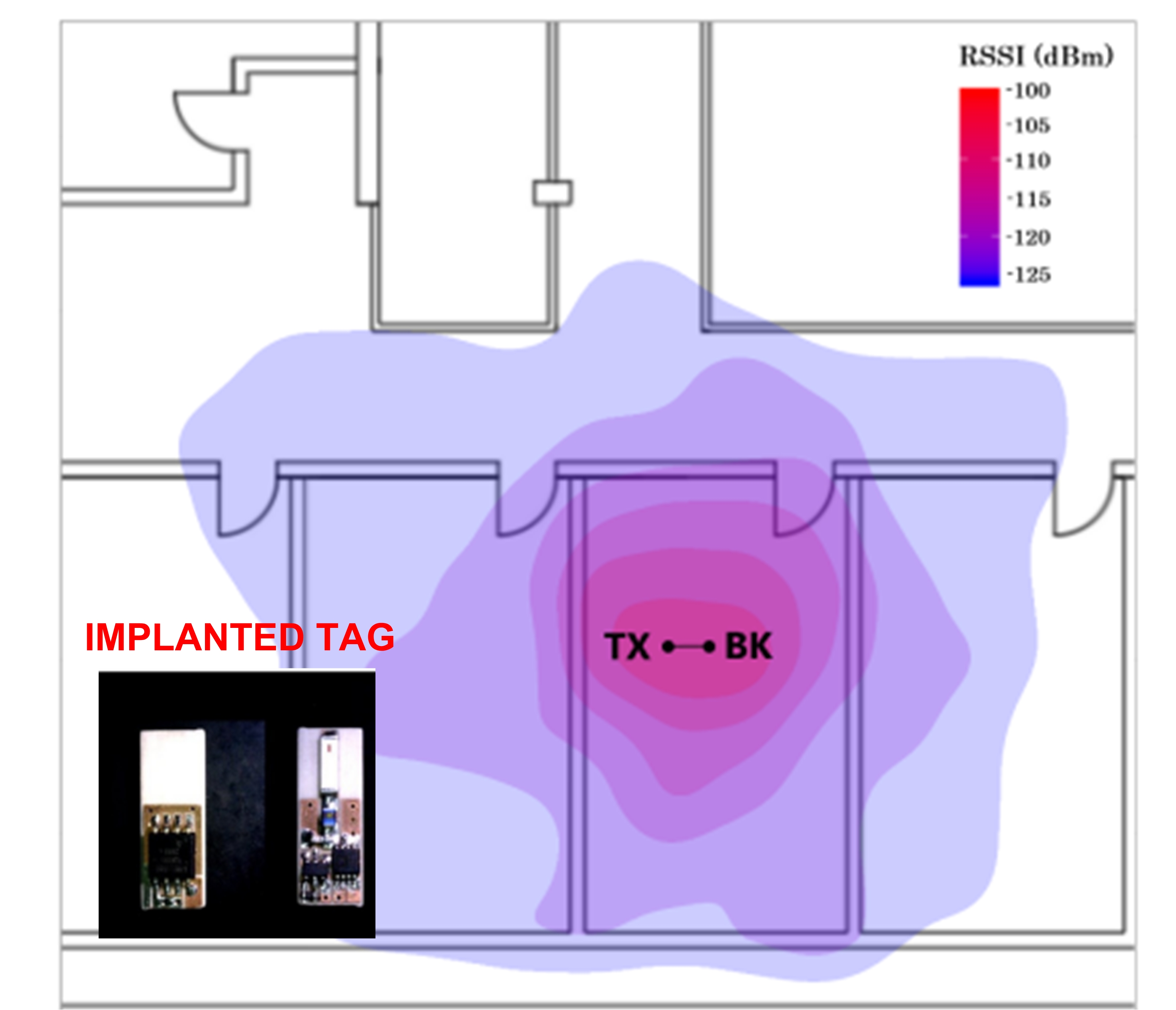
- Sensor networks with Zigbee, Bluetooth, LoRAN technology applied to radio communication of data from remote sensing biomedical systems, sensor networks for different applications (civil engineering, automotive, logistics sector, food sector, etc.) and the its integration into the IoT database.
- Integration of sensors (humidity, temperature, pH, biomedical, etc.) in passive and semi-passive RFID tags for applications wearables.
- Study of harvesting techniques to charge batteries from energy from the environment (RF, vibrations, thermal).
- Development of communications for backscatering using Software Defined Radio (SDR).
- 2 Development of microwave circuits and systems:
- Antenna design for RFID readers and mobile applications.
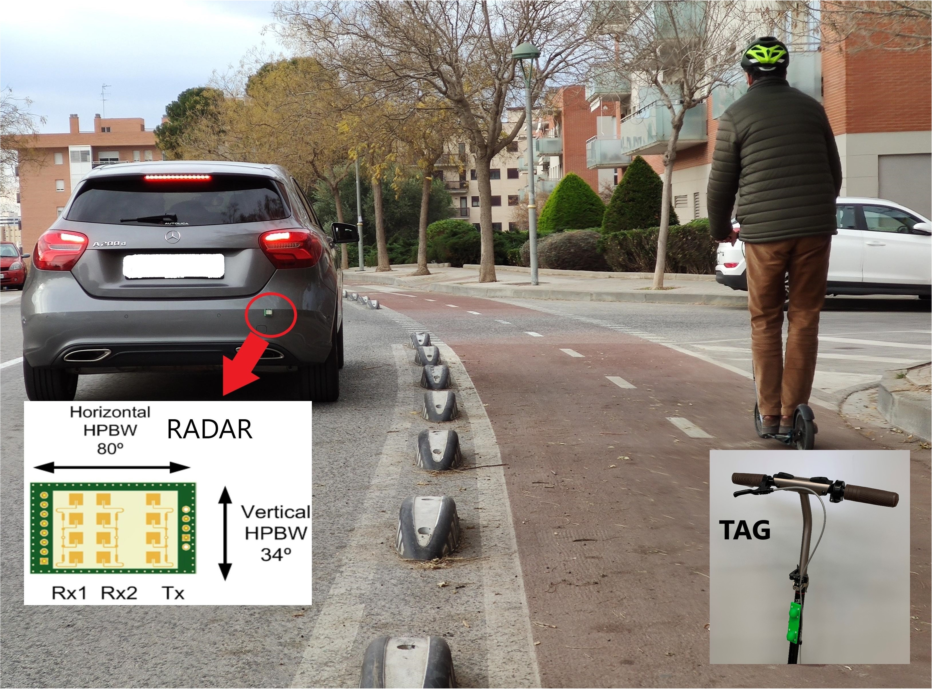
- Development of RADARS applications in millimeter band (24 GHz, 60 GHz and 77 GHz) for automotive and Smart IOT applications (gesture detection, presence, MMID).
- Models of microwave devices (transistors, diodes, MEMS devices).
